IBM Patents a Tapered Contact Structure for Next-Gen Nanosheet Transistors
As transistors shrink to nanosheet dimensions, the tiny metal contacts that carry current in and out become a serious engineering headache. IBM's latest patent describes a clever geometric fix — a contact that's wider at the bottom than the top — to solve the crowding problem without sacrificing performance.
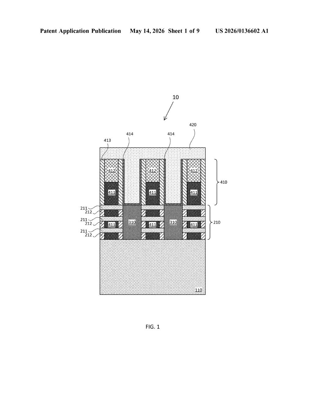
What IBM's T-shaped transistor contact actually does
Imagine a skyscraper where the lobby is wider than the floors above it. That's essentially what IBM is doing with the metal contacts inside its next-generation transistors. In a normal chip, these contacts are like little metal pillars that connect the transistor's active regions to the wiring above. Making them perfectly rectangular gets harder and harder as chips shrink.
IBM's patent describes a source/drain contact — the connector that links the transistor's current-carrying regions to the rest of the chip — that has a wider bottom section and a narrower top section. The bottom spreads out to make solid electrical contact with the transistor, while the narrower top avoids bumping into the metal gate sitting right next door.
This kind of geometry is called a mid-of-line (MOL) contact structure, and it's one of those invisible manufacturing details that determines whether a chip design actually works at cutting-edge scales. You'll never see it, but it affects how fast and energy-efficient your future devices could be.
How the wider bottom and narrower top solve a scaling problem
The patent covers a nanosheet transistor — a type of transistor where the channel (the part that switches current on and off) is a thin horizontal sheet of semiconductor material, stacked in layers. Nanosheets are the architecture Intel, TSMC, Samsung, and IBM are all racing toward for the most advanced chips.
The key innovation is the shape of the source/drain contact: it has a bottom portion that is wider in the gate-length direction and a top portion that is narrower. This inverted-trapezoid or T-like profile sits directly on top of the source/drain epitaxial region (the grown semiconductor material that feeds current into the channel).
Here's why the shape matters:
- Wider bottom: maximizes contact area with the source/drain region, reducing electrical resistance.
- Narrower top: keeps the contact from encroaching on the adjacent dielectric cap (an insulating layer sitting on top of the metal gate), which prevents short circuits.
- Dielectric cap protection: the cap on the gate acts as a hard stop during fabrication, helping define the contact's geometry precisely.
The method described involves selective etching and deposition steps that create this non-rectangular profile in the contact trench — something that becomes increasingly critical as the space between gate and contact shrinks below a few nanometers.
What this means for sub-2nm chip manufacturing
At the 2nm node and beyond, the gap between a transistor's gate and its source/drain contacts is measured in single-digit nanometers. A contact that's even slightly misaligned or too wide can short out the gate, killing the transistor. IBM's tapered geometry builds in a structural tolerance — the narrower top naturally stays away from the gate even if deposition isn't perfectly centered.
For chipmakers, this kind of process margin (wiggle room in manufacturing) is enormously valuable. It can mean the difference between acceptable yields and a fab line that produces mostly defective chips. If this contact geometry makes it into IBM's nanosheet process — or gets licensed to foundry partners — it could quietly improve the reliability of chips that end up in your phone, laptop, or data center.
This is deep-in-the-stack semiconductor process engineering — the kind of patent that matters enormously to a fab process team and is completely invisible to everyone else. It's not exciting to read about, but tapered contact geometries like this are exactly the type of incremental innovation that separates working chips from non-working ones at the frontier nodes. Worth tracking if you follow semiconductor process technology.
Get one Big Tech patent every Sunday
Plain English, intelligent commentary, no hype. Free.
Editorial commentary on a publicly published patent application. Not legal advice.