
Sony Patent Targets Noise Reduction Through Geometric Pixel Circuit Layout in Camera Sensors
Every camera sensor has a noise problem baked into its silicon, and Sony's latest patent targets that problem at the transistor level, using geometric symmetry to balance out the tiny electrical mismatches that make photos look grainy.
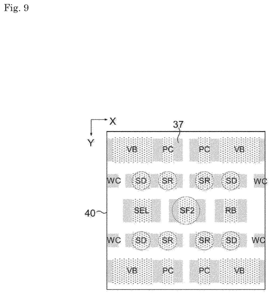
What Sony's symmetrical pixel layout actually does
Every time your phone snaps a photo, millions of tiny light-collecting cells have to be read out almost simultaneously, and the circuits doing that reading can introduce small errors that show up as grain or uneven color. The more cells you cram onto a sensor, the harder it gets to keep those errors equal across the whole frame.
Sony's patent describes a way of arranging the transistors that handle this readout job so that they sit in a mirror or rotational pattern around a central transistor. Because the surrounding parts are physically balanced, the tiny manufacturing imperfections that cause uneven readings tend to cancel each other out rather than pile up. Think of it like a perfectly balanced scale: any small weight you add to one side is matched by the same weight on the other.
The result is cleaner pixel data before any software processing even starts, which matters especially in low-light photos where noise is most visible.
… two or more of the first transistors and two or more of the second transistors included in the two or more first pixel circuits are arranged in point symmetry or line symmetry around the one third transistor.
Translation: The sensor components are laid out in a precise geometric pattern around a central transistor to reduce signal noise.
How the two-capacitor, shared-transistor design works
The patent describes a light detection device built around two layers of pixel circuits working together.
The first layer, called first pixel circuits, sits closest to the actual light-collecting elements. Each circuit grabs two voltage readings from its pixel: one taken when the pixel is reset (a baseline) and one taken after the light-generated charge has been read in. Storing both lets downstream electronics subtract the baseline from the signal reading, a classic noise-reduction trick called correlated double sampling. Each of those two readings is stored in a dedicated capacitor (a tiny charge-holding component), so neither is lost while the other is being processed.
The second layer, called second pixel circuits, is shared by two or more first pixel circuits. It includes a central source follower transistor (a component that converts stored charge into a measurable voltage) and reads out the first-layer capacitors one at a time into a shared node called the second floating diffusion region.
The key invention is the physical arrangement: the transfer transistors from all the first pixel circuits that feed into one second pixel circuit are placed in point symmetry or line symmetry around that central source follower transistor. Because symmetric transistors on a chip experience nearly identical manufacturing conditions, their electrical characteristics match closely, reducing the mismatch errors that would otherwise appear as fixed-pattern noise across the image.
… a plurality of second pixel circuits that are shared by each of two or more first pixel circuits, each second pixel circuit includes: a first capacitive element; a second capacitive element; a first transistor configured to switch between whether or not to transfer an electric charge …
Translation: The design allows multiple pixel circuits to share components, using specific switches to manage the flow of electricity.
What this means for Sony's image sensor business
For Sony, image sensors are a core business, supplying chips to smartphone makers, camera brands, and automotive camera systems. Noise performance at the pixel-circuit level is one of the primary battlegrounds in that market, and improvements here can justify premium pricing without requiring a bigger sensor or a longer exposure time. A design that reduces fixed-pattern noise structurally (rather than through software correction after the fact) means less computational work and cleaner output in real-time applications like video and machine vision.
The filing sits squarely in the chip-architecture corner of the latest Big Tech patents covering image sensor design, where incremental layout decisions can compound into meaningful real-world differences in photo quality and sensor yield at the factory.
Sony's 359th filing among the patents we've tracked since May in our Sony coverage joins earlier applications like a cross-network device readings system and an automatic scene layout mapper.
The patent protects one very specific thing: the exact geometric pattern Sony uses to arrange transistors on a chip. Think of it like copyrighting a particular floor plan for a house, not the idea of houses in general. A rival company could simply draw a different floor plan and walk right around this protection.
That limits how much this patent can actually block competitors. The core ideas behind Sony's noise-reduction method have been around for years and belong to no one. Sony's real gain here is narrower but still useful. They have locked down their own proven blueprint on paper, making it harder for anyone to copy their exact physical design outright.
Get our take in your Top Stories
Liked this breakdown? Add Patentlyze as a preferred source on Google, and our plain-English take shows up more often in your Top Stories the next time Sony patent news breaks.
There are more where this came from
We read every patent application Big Tech publishes and send you the ones worth knowing. Plain English, free, every week.
The drawings
57 drawing sheets from US 2026/0247049 A1 · click any drawing to enlarge


Want this weekly breakdown for a company we don't cover? Patentlyze Pro →
Be the first to weigh in