Qualcomm Patents a Way to Bundle Matrix Math Instructions Before They Hit the Accelerator
Every time a CPU fires an instruction at a hardware accelerator, there's overhead in the handoff. Qualcomm's new patent is about collapsing multiple matrix math requests into a single packet before they ever leave the CPU — a small idea with real throughput implications.
What Qualcomm's instruction-batching trick actually does
Imagine you're sending packages one at a time across town, when you could just wait two minutes and stuff them all into one truck. That's essentially the inefficiency this patent addresses.
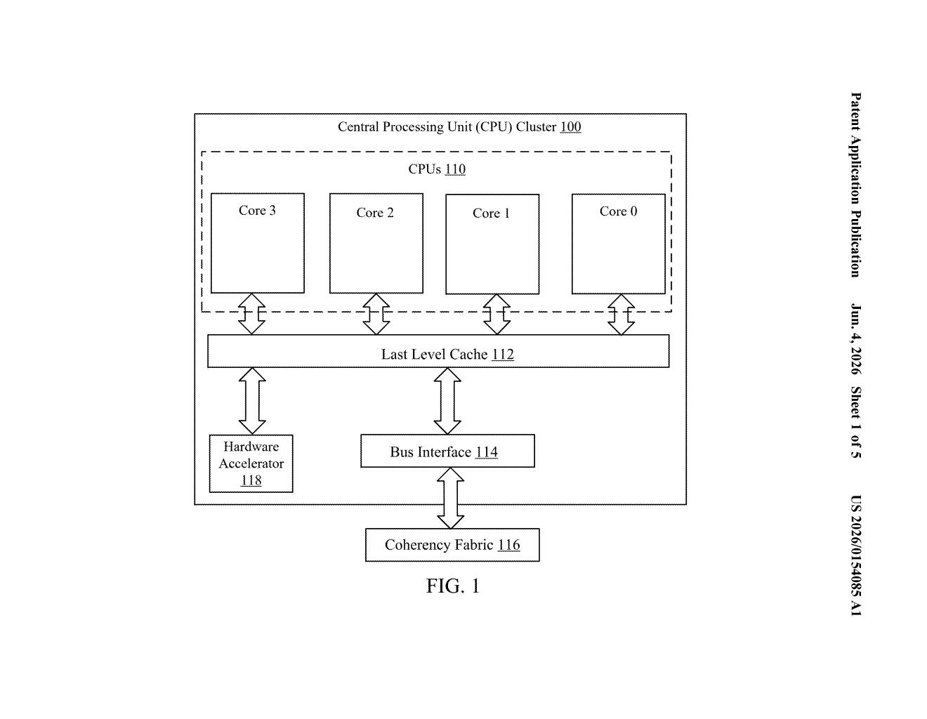
When your phone or laptop runs AI tasks, the main CPU regularly sends instructions to a dedicated math accelerator — a specialized chip good at the matrix multiplications that power things like speech recognition or image processing. Normally, each instruction gets sent individually, which creates a steady stream of small, chatty handoffs.
Qualcomm's idea is to hold those instructions briefly in a small buffer on the CPU side, merge two or more of them into a single bundled packet, and then send the whole thing to the accelerator at once. Fewer trips, more work per trip — the accelerator stays busier, and the connection between CPU and accelerator gets used more efficiently.
How the CPU buffer merges SME requests into packets
The patent specifically targets Scalable Matrix Extension (SME) requests — SME is an Arm architecture feature that lets a CPU offload large matrix math operations, the kind used heavily in machine learning inference.
The mechanism works like this:
- The CPU receives a first SME request and parks it in an internal buffer rather than immediately forwarding it.
- A second SME request arrives and is also held in the same buffer.
- The buffer logic merges the two requests into a single request packet.
- That consolidated packet is sent to the hardware accelerator in one transaction.
The key insight is reducing the number of individual transactions crossing the CPU-to-accelerator interface. Each crossing has fixed overhead — protocol framing, bus arbitration, handshaking — so cutting the number of crossings directly reduces wasted cycles.
This is a form of instruction coalescing (the same idea used in GPU memory systems, where scattered memory reads get bundled into fewer, wider requests). Qualcomm is applying it to the control path between a CPU core and its paired accelerator.
What this means for AI chip efficiency on Qualcomm silicon
On-device AI inference is gated by how efficiently the CPU can feed work to its accelerators. If the CPU is constantly trickling individual matrix requests, the accelerator spends time waiting rather than computing — a classic bandwidth starvation problem. Batching at the buffer level is a low-latency fix that doesn't require changing the accelerator hardware itself.
For Qualcomm specifically, this kind of optimization matters for the Snapdragon family, where an Arm CPU cluster sits alongside an NPU (neural processing unit). Squeezing more instruction throughput through that interface means faster AI task completion and, in mobile contexts, potentially better energy efficiency — since the accelerator finishes its work and can power down sooner.
This is unglamorous plumbing work, but it's the kind of micro-optimization that actually moves benchmark numbers on production silicon. Instruction coalescing is a well-understood technique in GPU and memory controller design — applying it explicitly to CPU-to-accelerator SME traffic is a focused, practical improvement. It won't generate headlines at a product launch, but it's the sort of thing that shows up as a few percentage points of AI inference throughput across every Snapdragon device that ships with it.
Get one Big Tech patent every Sunday
Plain English, intelligent commentary, no hype. Free.
Editorial commentary on a publicly published patent application. Not legal advice.