Samsung Patents a Multi-Adhesive Layer Design for Stacked Semiconductor Packages
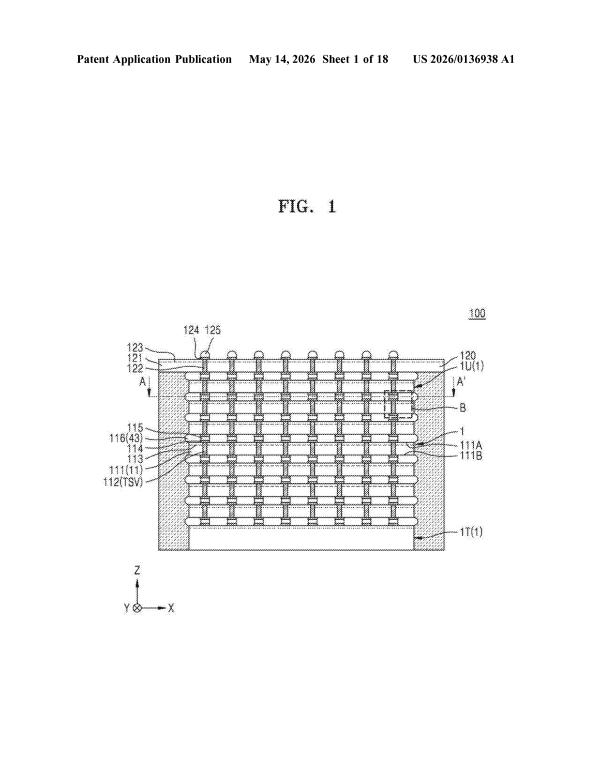
Stacking memory chips sounds simple until you realize that keeping them mechanically stable, thermally compliant, and electrically connected at microscopic scales is…

From processors and AI accelerators to the packaging and cooling that hold them together, this is where the silicon race lives. Every chip filing, decoded without the jargon.
Stacking memory chips sounds simple until you realize that keeping them mechanically stable, thermally compliant, and electrically connected at microscopic scales is…
Samsung is patenting a transistor architecture where stacked semiconductor layers deliberately vary in thickness — a structural tweak that could influence how…
Building a chip is extraordinarily sensitive — tiny variations in temperature, pressure, or chemistry during fabrication can silently degrade a product that…
Samsung is patenting a transistor design that stacks multiple 2D semiconductor channels — like sheets of atomically thin material — both horizontally…
Cracks in semiconductor chips aren't just cosmetic — they can silently kill a device long after it leaves the factory. Samsung's latest…
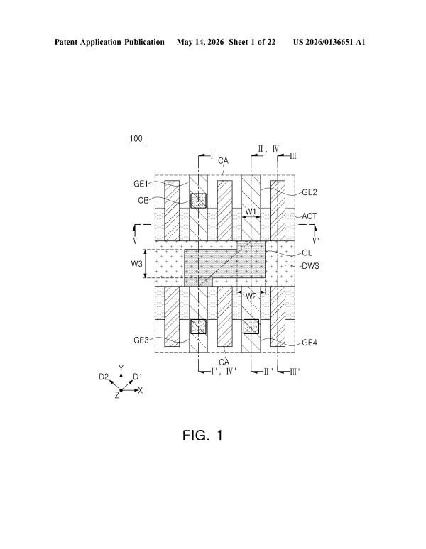
Samsung is patenting a clever structural trick that electrically ties together gate electrodes sitting on opposite sides of an isolation wall —…
Chip manufacturing lives or dies on coating uniformity — and Samsung's latest patent targets a surprisingly overlooked weak point: the magnetic field…
As chips shrink to atomic scales, routing electrical connections between transistors becomes a puzzle in three dimensions. Samsung's latest patent tackles exactly…
Samsung is filing patents on a packaging technique that buries capacitors inside the circuit substrate itself — not on top of it…
As memory chips get denser and more three-dimensional, the manufacturing steps used to etch one part of the chip can accidentally damage…
Samsung is filing patents on a way to stack two sets of transistors on top of each other, separated by a special…
Samsung is working on a way to keep ultra-thin, atom-scale semiconductor channels from peeling off their substrates — a surprisingly tricky problem…
We read every patent application Big Tech publishes and send you the ones worth knowing. Plain English, free, every week.