
Nvidia Files Patent for an AI Chip Stacked on Memory to Cut Chatbot Lag
Nvidia's filing describes an AI chip that sits directly on top of its memory, so the data a chatbot needs is a short hop away instead of a long trip. The chip also passes results between its own parts on pre-set routes, without parking them in shared storage first.
What Nvidia's memory-stacked AI chip does
Imagine asking an AI assistant a question and watching it type out the answer one word at a time, pausing between words. Part of that delay comes from the chip fetching data from memory and passing notes between its own parts.
Nvidia's filing describes a chip built to cut those trips. Instead of sitting beside its memory, the chip is stacked directly on memory chips, so data has a short path. Inside, one group of small processing blocks does the math in pieces, and another group combines those pieces into a finished answer for each step.
The pieces travel over a wiring network that is set up in advance for the specific AI model. Results go straight from one block to the next instead of being dropped into a shared storage area first.
transmitting, by one or more compute tiles fabricated in the LLI device, a read request generated by one or more memory read interfaces within the one or more compute tiles via first electrical contacts to the one or more memory dies to retrieve one or more tensor inputs stored in the one or more memory dies; …
Translation: The chip's processing units send read requests directly into the adjacent memory layers to pull in stored data.
How the chip's tiles pass partial answers along
The filing covers a method for doing the core math of an AI model on a chip that is stacked with one or more memory chips (the claims call it a low-latency inference, or LLI, device). Electrical contacts line up between the layers, so the processor reads its inputs from memory and writes finished results back over short, direct connections.
The work is split between two kinds of blocks:
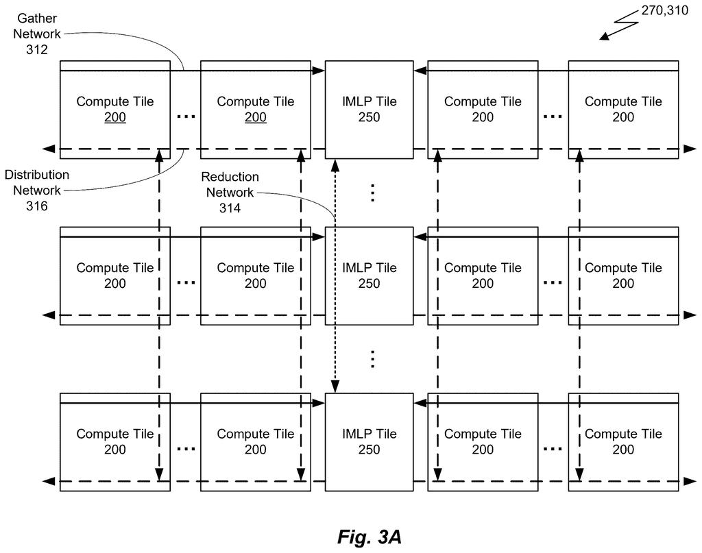
- Compute tiles read the model's numbers from memory and do matrix math (multiplying big grids of numbers), producing partial results.
- Inter-matrix layer processing (IMLP) tiles add those partial pieces into reduced results, handle steps like normalizing values, and write the finished answer back to memory.
A configurable network links the tiles. It has a gather network (pieces go to an IMLP tile), a reduction network (IMLP tiles combine their results), and a distribution network (answers are broadcast back to compute tiles). The connections are pre-configured for the model being run, and partial results move tile to tile without being stored in the stacked memory.
The memory also holds the KV cache (the running notes a model keeps about your conversation so far). The filing describes boards of 24 such chips and racks of boards, and puts the chip on top of the memory so more of its surface can shed heat.
The low-latency inference device may be stacked with one or more memory die for storing tensor inputs, KV cache data, activations, and other neural network-related information required for inference.
Translation: Placing the AI chip directly on top of memory dies keeps chat history and model data close at hand to speed up responses.
Why faster chatbot replies depend on memory
If you use a chatbot, voice assistant or live translator, part of the wait between your question and the answer comes from chips shuffling data around. A design that keeps data close and skips parking results in shared memory could shorten that wait and cut the power a data center burns doing it. The filing lists language models, self-driving simulation and AR among possible uses, though its detailed examples center on language models.
In the filing's example system, regular graphics processors handle reading your prompt while these chips generate the reply one word at a time. That split shows how Nvidia is thinking about dividing inference work between different kinds of hardware. Whether it ever ships is unknown, since a patent application describes a design, not a product.
Nvidia's 53rd filing we've tracked in the AI chip wars since July builds on one cutting data shuffling and one on shared chip memory.
The big trade here is flexibility for speed. Wiring the chip's pathways in advance for one specific AI model removes a lot of waiting, but it also builds the chip around a known recipe. If the models change shape, the chip needs new setup, and a pre-planned route cannot adapt on the fly the way a general-purpose chip can.
Stacking the chip on memory has its own cost: heat. Piling chips on top of each other makes warmth harder to get out, and the filing puts the compute layer on top so more of its surface can cool off. That helps, and it also limits how hot the chip can run.
The trade reads as worth it for one job: answering chatbot prompts quickly in a data center, where the same models run all day. For anything else, expect a narrower tool than a regular graphics chip.
Get our take in your Top Stories
Liked this breakdown? Add Patentlyze as a preferred source on Google, and our plain-English take shows up more often in your Top Stories the next time Nvidia patent news breaks.
There are more where this came from
We read every patent application Big Tech publishes and send you the ones worth knowing. Plain English, free, every week.
The drawings
37 drawing sheets from US 2026/0330261 A1 · click any drawing to enlarge


Show the other 29 sheets


Want this weekly breakdown for a company we don't cover? Patentlyze Pro →
Be the first to weigh in