
Nvidia Files Patent for a Chip That Gathers, Combines and Shares Partial AI Results
Nvidia's patent application sketches a chip that skips the memory trips slowing down chatbot answers, wiring results straight from one small math block to the next.
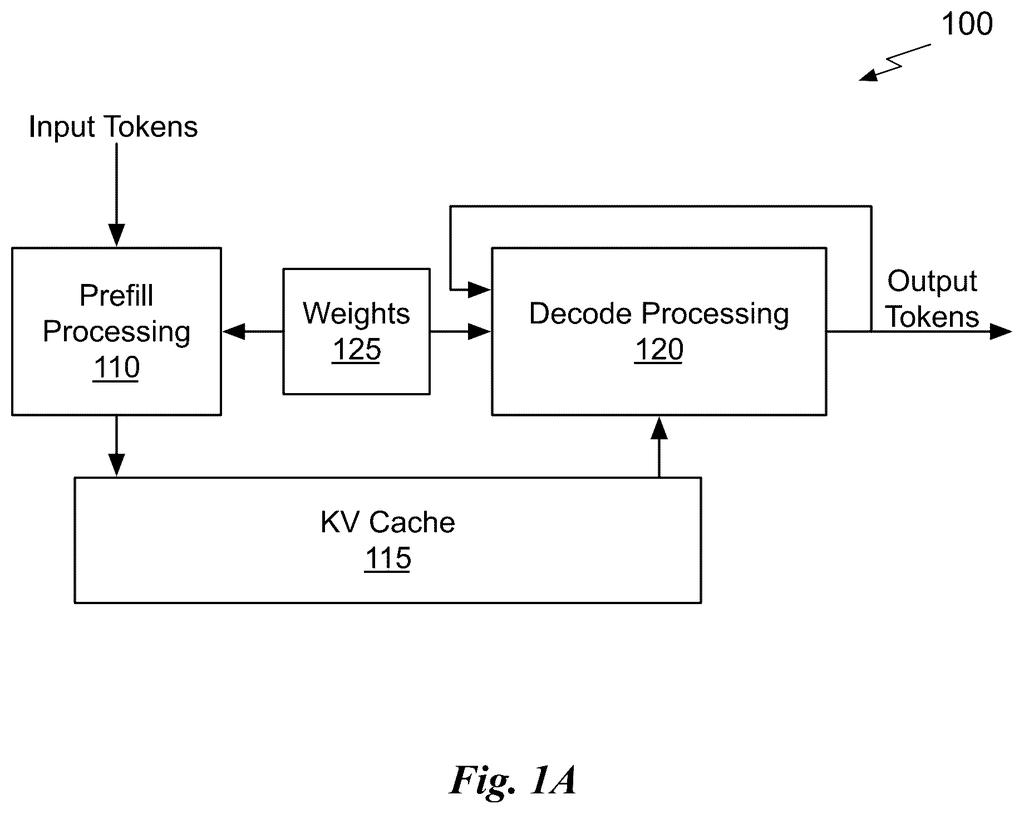
What Nvidia's chatbot-speed chip actually does
Ever noticed a chatbot typing its answer out one word at a time? That slow trickle has a cause. Behind each new word, the AI has to run through dozens of layers of math, and the chip doing the work keeps fetching the same stored numbers from memory.
Nvidia's patent application describes a chip built to cut those trips. Instead of one big pool of memory, it uses lots of small math blocks that each keep their own memory right beside them. Each block works out a piece of the answer. The pieces are then combined along dedicated wires and sent straight to the next blocks that need them.
Think of a kitchen where every cook has ingredients at their elbow, rather than one pantry down the hall. The filing says this setup cuts waiting time and energy use, which matters when millions of people are asking questions at once.
… transmitting, via a gather network, the plurality of partial results to an inter-matrix layer processing (IMLP) tile; generating, by the IMLP tile and based on the plurality of partial results, a local reduction result; …
Translation: It moves partial answers to a special processing tile to combine them.
How three separate wire networks pass results
Chatbots build an answer one small piece of text at a time, and each piece runs through every layer of the model (the filing mentions 80 or more layers for a model like Llama 70B). The filing proposes splitting the job: ordinary GPU boards read your prompt, and boards of these new chips handle the word-by-word part, called decoding.
The chip has two kinds of blocks. Compute tiles hold arrays of basic units, each with local SRAM (fast memory on the chip), vector registers (tiny scratch storage) and MAC units (circuits that multiply and add, the core math of AI). IMLP tiles (inter-matrix layer processing) combine partial answers and handle follow-up steps like normalization and softmax (rescaling numbers so they behave).
The first independent claim covers three steps, each with its own network:
- Gather: compute tiles in a group send partial results to their IMLP tile.
- Reduce: IMLP tiles combine those into a local result, pass it to another IMLP tile, and a global result comes back.
- Distribute: the final result, split into chunks called subvectors, is broadcast to compute tiles for the next step.
The three networks are physically separate and pipelined. They are set up ahead of time for the model being run, and the reduction network can be a tree or a chain. A second independent claim adds crossbar switches (grids that link any input to any output) and demultiplexers (switches that route one stream to many places) that deliver results into the right registers.
Each compute tile includes an array of basic units equipped with local SRAM, vector registers, and multiply-accumulate (MAC) units, enabling localized computation to minimize data movement and reduce latency.
Translation: Tiny local memory blocks keep data close by to speed up math tasks.
Why Nvidia's decode chip idea matters for chatbots
If this approach works, the practical payoff is chatbots, voice assistants and live translation that respond faster while using less electricity in the data centers behind them. The filing says the speedup comes from cutting repeated trips to a central memory, which is where much of the waiting happens today.
The filing also pairs these chips with GPU boards: GPUs read your prompt, and boards of 24 of the new chips (in a 4 by 6 grid) generate the reply, linked by NVLink, Nvidia's high-speed connection. That is a design for racks of servers, not your laptop. The text gives no speed numbers and does not say a product exists, so treat it as an engineering direction.
Nvidia's 59th filing we've tracked since July in our AI chip wars watchlist follows patents like one to speed chip sorting and one to cut chatbot wait times.
Chatbot lag is a small annoyance for you and a large expense for the companies running these models for millions of people. The filing's own numbers show why: a big model can have 80 layers or more, and every new word means passing through all of them while pulling the model's stored values from memory again.
Rebuilding the chip around that bottleneck matches the size of the problem. Rather than patching around slow memory trips, the design removes most of them by giving each small compute block its own memory and wiring results straight to where they are needed next.
The wiring is set ahead of time for a particular model, which fits big data center deployments. The filing gives no speed results, so how much faster it gets stays unproven.
Get our take in your Top Stories
Liked this breakdown? Add Patentlyze as a preferred source on Google, and our plain-English take shows up more often in your Top Stories the next time Nvidia patent news breaks.
There are more where this came from
We read every patent application Big Tech publishes and send you the ones worth knowing. Plain English, free, every week.
The drawings
22 drawing sheets from US 2026/0329803 A1 · click any drawing to enlarge


Show the other 14 sheets


Want this weekly breakdown for a company we don't cover? Patentlyze Pro →
Be the first to weigh in