
Nvidia Files Patent for a Chip Built to Cut the Wait on Chatbot Replies
Nvidia's filing sketches a chip for writing chatbot answers where each step's results skip shared memory entirely. They travel straight, along wiring planned ahead of time, to the block that needs them next.
What Nvidia's low-latency chatbot chip does
When a chatbot writes its answer one word at a time, the computer behind it runs the job through dozens of layers for every single word. A model like Llama 70B has 80 or more of them. On today's graphics chips, each layer's results get shuffled through a central memory before the next layer can start, and all that shuffling adds up to a lag you can feel.
Nvidia's filing describes a different chip layout for the answer-writing half of the job. Instead of one big shared memory, the chip is split into many small blocks, each with its own storage sitting right next to its math circuits. When a block finishes, a network of wires set up in advance sends the result straight to whichever block needs it next.
The route is planned before the chatbot ever runs, so nothing waits around to be told where to go. The filing pairs these chips with regular Nvidia GPUs, which handle reading your prompt while the new chips write the reply.
… determining a mapping of IMLP tiles to compute tiles based on the first spatial distribution and the second spatial distribution; performing the first BMM operation to calculate dot-product attention scores for one or more attention heads of the LLM …
Translation: The chip figures out how to route data between its processing units to quickly calculate the attention scores chatbots need.
How the chip's tiles hand off attention scores
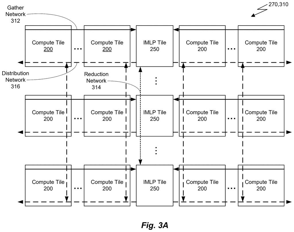
The claims cover how a chatbot's decode step (the part that writes the answer one word at a time) is spread over a grid of small processing blocks called compute tiles. Tiles are organized into groups, and each group has one extra helper block, an IMLP tile, that combines partial results and does the cleanup math between layers.
Inside each compute tile are small units with their own memory, a few registers, and multiply-and-add circuits, so the stored model numbers never travel far. The attention step (where the model weighs how much each earlier word matters) runs as two big batches of multiplication:
- First, the new word's query is multiplied by stored key data to produce attention scores.
- The helper blocks then normalize those scores (turn them into shares that add up to one) and hand slices of them back to the compute tiles.
- Second, the normalized scores are multiplied by stored value data to get a weighted sum.
A controller decides in advance how each multiplication is split across the tile groups and which helper block feeds which compute tile. It then sets up a configurable network so slices go directly from a source register to a destination register. The same pattern repeats for the fully connected layers that follow.
Compute tiles are configured to efficiently execute matrix operations in parallel. Each compute tile includes an array of basic units equipped with local SRAM, vector registers, and multiply-accumulate (MAC) units, enabling localized computation to minimize data movement and reduce latency.
Translation: Mini processors use local memory and math units to crunch numbers right where they sit, which avoids slow data transfers.
What this means for chatbot response times
If this design works, the practical payoff is chatbot replies that start arriving sooner and keep flowing faster, especially when a lot of people are using the same service. The filing points to uses such as voice assistants, real-time translation, driving and robots, all places where a pause feels awkward or even unsafe.
The filing also describes pairing Nvidia's familiar graphics processors with separate answer-writing chips on boards linked together by NVLink connections. You would never buy one of these chips yourself, but you could notice it as a chatbot that responds with less lag. The filing also claims lower energy use, because less data has to travel long distances across the chip.
Nvidia's 57th filing we've tracked in our AI chip wars watchlist since July adds to a run that includes one on faster chatbot replies and another on reply-speed hardware.
Every speed trick here costs flexibility. Because the wiring between blocks is planned before the chatbot runs, the chip works best when it knows the exact shape of the model it will serve. The filing admits this by adding a second network for traffic that cannot be predicted ahead of time.
There is a second cost in memory. Each block keeps its own storage right beside its math circuits, which makes data fast to reach but means a big model has to be spread over many chips, boards and racks. That is a lot of hardware for one job, and it only handles the answer-writing half, so regular GPUs still have to read your prompt first.
The trade looks worth it for a company serving millions of chat requests where every fraction of a second counts. It looks risky if chatbot designs change faster than chips can be built, though the filing's programmable tiles are a reasonable hedge against that.
Get our take in your Top Stories
Liked this breakdown? Add Patentlyze as a preferred source on Google, and our plain-English take shows up more often in your Top Stories the next time Nvidia patent news breaks.
There are more where this came from
We read every patent application Big Tech publishes and send you the ones worth knowing. Plain English, free, every week.
The drawings
22 drawing sheets from US 2026/0330199 A1 · click any drawing to enlarge


Show the other 14 sheets


Want this weekly breakdown for a company we don't cover? Patentlyze Pro →
Be the first to weigh in