
Nvidia Files Patent for AI Chip Tiles With Memory Wired Right Beside the Math
Every word a chatbot writes means pushing numbers through dozens of layers of math, and a lot of the delay comes from shuttling those numbers around. Nvidia's patent application redesigns the chip so each step hands its result straight to the next.
What Nvidia's chatbot-speed chip design does
Ever watched a chatbot type out an answer one word at a time? Behind each word, the computer runs your question through dozens of layers of math, 80 or more in a big model like Llama 70B. Today's graphics chips do that math fast, but they spend a lot of time shuttling numbers back and forth to a shared memory bank between steps.
Nvidia's patent application describes a chip built for that one job. Each small block of the chip keeps its own memory right beside its own math circuits, so the numbers it needs are already close by. It's like a kitchen where every cook has a pantry at their elbow instead of sharing one across the building.
When a block finishes, its result goes straight to whichever block needs it next, along wiring planned ahead for that particular AI model.
shared control logic that configures the set of gather groups to process inputs in parallel; reduction and element-wise computation logic; and an array of basic units, each basic unit comprising: RAM; and arithmetic logic directly coupled to the RAM; …
Translation: The chip uses closely linked memory and math units to process information simultaneously.
How tiles hand results straight to each other
The claims cover a method for running the heavy math behind an AI model's answer (the filing calls this low latency inference, meaning generating output with as little waiting as possible). Inputs are spread across gather groups, and each group holds several compute tiles.
Inside a tile is a grid of basic units. Each one has its own local memory (SRAM), a few small scratch registers, and multiply-accumulate circuits (the part that multiplies numbers and adds them up, the core move in AI math) sitting directly against that memory. Shared control logic tells every unit to work in parallel, and reduction logic in the tile adds their partial answers into one result for the group.
The description adds the rest of the flow:
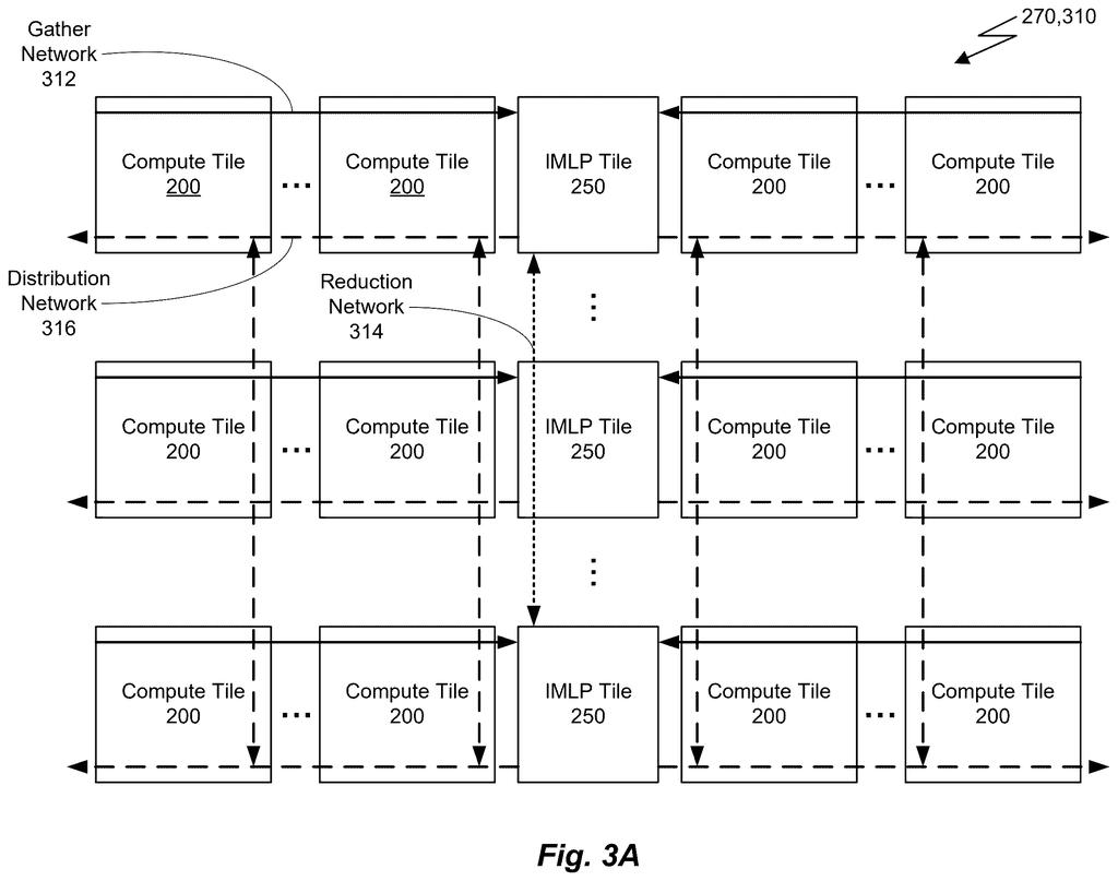
- Gather: tiles send partial results to a helper tile (an IMLP tile) that sums them and handles steps like normalizing.
- Reduce: helper tiles combine results across groups in a tree shape.
- Distribute: final results are broadcast straight into the registers of the tiles that need them next.
Those routes are set in advance for the model being run, so nothing stops at shared memory. In the example setup, GPUs read your prompt while boards of these chips (24 per board, in a 4 by 6 grid) generate the reply. The filing even shows a timeline where one step, softmax (a score-normalizing step in attention), is completely hidden behind other work.
Each compute tile includes an array of basic units equipped with local SRAM, vector registers, and multiply-accumulate (MAC) units, enabling localized computation to minimize data movement and reduce latency.
Translation: Keeping memory right next to the processor helps the chip reply much faster.
Why Nvidia is rethinking chips for chatbot replies
If this design ever reached real hardware, the payoff would show up as chatbot and voice assistant replies that start and finish sooner. The filing names virtual assistants, real-time translation, robots and autonomous driving as uses that can't tolerate lag.
It also points to energy. Fewer trips to big memory means less power burned per answer, which adds up in data centers serving millions of people at once. Keep in mind this is a patent application describing a design on paper, and GPUs still handle the prompt-reading step in the setup it lays out.
Nvidia's 55th filing we've tracked in our AI chip wars watch since July adds to a run that includes shrinking language models and stacking chips on memory.
If you use a chatbot or a voice assistant, the delay you feel before the first word and between words is exactly what this design goes after. You would never see the chip itself. You would only notice replies that arrive with less of that awkward pause.
Whether that happens depends on numbers the text we reviewed does not give: there is no side-by-side speed test against today's chips, only design figures like tile counts and cycle counts. Still, the aim matches a real annoyance, and handing results from tile to tile without a memory stop is a sensible way to attack it.
For you, the realistic timeline is long and indirect, since this hardware would sit in data centers first. A filing is a design on paper, and the benefit arrives only if someone builds it and offers a service on top.
Get our take in your Top Stories
Liked this breakdown? Add Patentlyze as a preferred source on Google, and our plain-English take shows up more often in your Top Stories the next time Nvidia patent news breaks.
There are more where this came from
We read every patent application Big Tech publishes and send you the ones worth knowing. Plain English, free, every week.
The drawings
22 drawing sheets from US 2026/0330206 A1 · click any drawing to enlarge


Show the other 14 sheets


Want this weekly breakdown for a company we don't cover? Patentlyze Pro →
Be the first to weigh in