
Samsung Patents a Mobile Chip That Splits AI Work Across Two Processors
Samsung has filed a patent for a chip architecture that splits AI calculations between two separate processors sitting in the same mobile device, letting both work in parallel instead of waiting in line.
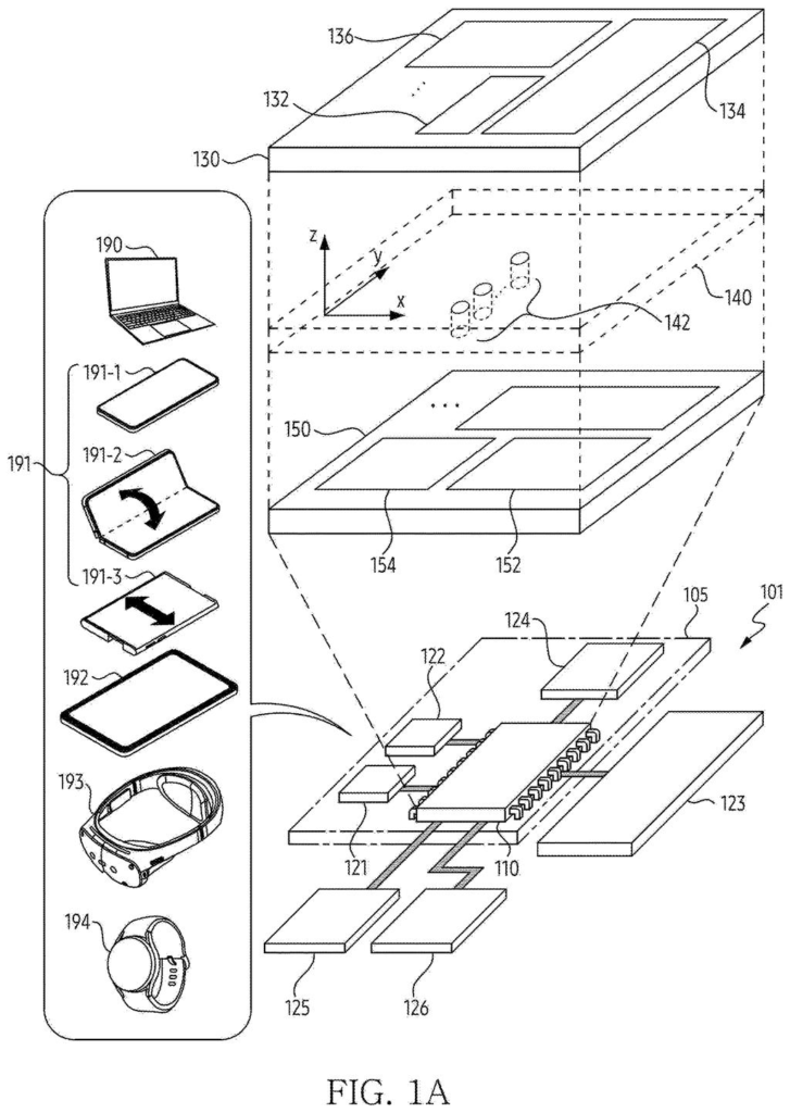
How Samsung's split-processing chip handles AI on phones
A phone's AI chip grinds through a photo, a voice command, or a translation request one step at a time. The chip gets the whole job, does it start to finish, and every other task waits. That bottleneck is what Samsung's new patent is trying to fix.
The idea is to split the work. A helper processor called a DMA processor (think of it as a relay runner) handles one chunk of the calculation. At the same time, it hands off the remaining data to the main AI chip so that chip can work on its own portion. Both legs of the race happen together instead of one after the other.
For you, the goal is simple: AI tasks on your phone (real-time translation, photo enhancement, voice recognition) finish faster, without draining the main processor. The design keeps the heavy lifter free for the next job rather than tying it up start to finish.
… at least one direct memory access (DMA) processor positioned outside the processing circuitry communicatively coupled to the processing circuitry and the memory …
Translation: An extra data processor sits outside the main chip to help handle tasks.
How the DMA processor and NPU divide a neural-network task
The patent describes a mobile chip stack built from two dies (separate silicon layers bonded together). The top die holds the NPU (neural processing unit, the chip dedicated to AI math). The bottom die holds cache memory and a DMA controller (Direct Memory Access controller, a circuit that moves data independently without burdening the main processor).
The two dies communicate through TSVs (through-silicon vias, essentially tiny vertical wires drilled through the chip layers) connected to a bus interface. This physical link is what makes the split-processing trick possible.
When the device runs a neural-network task, the workload is divided into two portions:
- The DMA processor takes portion A and runs its computation independently.
- While that is happening, the result or the remaining data (portion B) is sent over the TSV bus to the NPU on the other die.
- The NPU completes the second computation, then writes the final result to main memory.
The first independent claim expands this to any mobile communication device: the DMA processor sits outside the main processing circuitry, handles the first computation, then passes its result back. The processing circuitry finishes the second computation. The key word in the claim is parallel: the point is not just splitting work but overlapping it in time.
… a first die including a neural processing unit (NPU) circuit, a second die including cache memory and direct memory access (DMA) controller for data communication …
Translation: The chip is split into two layers, one for AI tasks and another for data movement.
What faster on-device AI could mean for your phone
Most phone AI chips today run neural-network layers sequentially, which means the main processor is busy for the entire duration of a task. A design that hands off part of the work to a dedicated DMA processor could reduce how long the NPU is tied up, leaving it free to start the next request sooner. For on-device AI features like live camera processing or real-time translation, that freed time could close the gap between what a phone does today and what people currently expect a cloud server to do.
Samsung has been filing around on-device AI processing since 2024, and this patent is a step deeper into that territory. Whether the specific two-die, TSV-connected design reaches mass production is a separate question, but the direction is clear: Samsung is trying to make AI work feel instantaneous on hardware that fits in your pocket.
Samsung's 53rd filing we've tracked since June in the AI chip wars builds on earlier applications, including one fixing signal reception and one cutting idle power.
The AI tasks your phone handles every day, things like cleaning up a photo, translating a conversation in real time, or drafting a quick reply, are about to get noticeably faster and easier on your battery. Samsung's design gives a dedicated layer of the chip the ability to do part of the AI work itself, so by the time the main processor takes over, a chunk of the job is already done.
The practical result is fewer of those small but annoying moments where you wait for the phone to catch up to you.
There is one honest condition: this only speeds things up in apps that are built to use the new workflow, so the benefit arrives gradually as developers update their software rather than all at once when you upgrade your phone.
There are more where this came from
We read every patent application Big Tech publishes and send you the ones worth knowing. Plain English, free, every week.
The drawings
13 drawing sheets from US 2026/0277834 A1 · click any drawing to enlarge


Want this weekly breakdown for a company we don't cover? Patentlyze Pro →