
Samsung Patents a Fix That Makes Gaps Between Joined Screens Invisible
Every time display makers bolt two screens together, they face the same headache: the seam between panels looks brighter or dimmer than the rest of the image. Samsung's new patent tackles that with a resin layer whose optical properties are tuned to make the boundary nearly invisible.
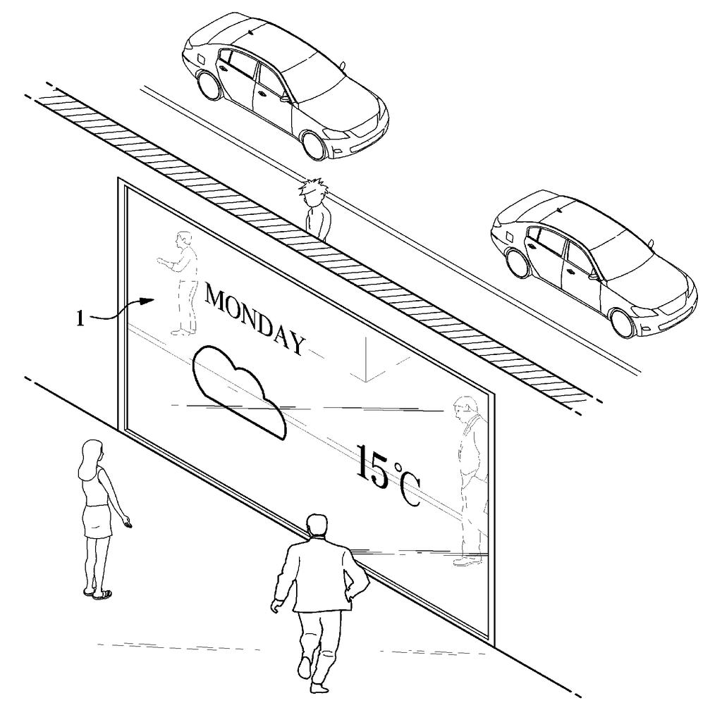
What Samsung's panel-seam resin layer actually does
Ever stared at a big mall screen or a fancy TV wall and noticed a faint line where two panels meet? That line exists because light behaves slightly differently the moment it crosses from one material to another, and the gap between panels is exactly the wrong place for that to happen.
Samsung's patent describes filling that gap with a special resin, a transparent glue-like material, whose light-bending properties are calibrated so that the brightness difference between light going in and light coming out stays below a detectable limit. The goal is that your eye never registers a seam at all.
The patent also covers adjusting the brightness of the individual LEDs closest to the boundary, so both the physical gap and the electrical output at the edges are working together to sell the illusion of one continuous image.
… the resin layer has a refractive index such that a difference between the refractive index of the resin layer and a reference refractive index is within a range in which a change in luminance between light incident on the display apparatus and light passing through the display apparatus is minimized …
Translation: The gap is filled with a special material that bends light to hide the seam between the two screens.
How the refractive index keeps light consistent at the join
The core idea is controlling the refractive index of a resin layer placed between two adjacent display modules. Refractive index is simply a number that describes how much a material bends or slows light; the closer two materials' refractive indices are, the less light scatters or dims at their boundary.
Samsung's patent specifies that the resin's refractive index must differ from a reference value by no more than the amount that keeps luminance change (brightness shift) below a predetermined threshold. In plain terms: the resin is chosen so that light crossing the seam looks essentially identical to light anywhere else on the screen.
The patent pairs this optical fix with a software-side control layer:
- Pixels near the boundary are identified as boundary pixels on both modules.
- Each boundary pixel contains multiple LEDs, including one closer to the seam and one further away, each emitting a different color.
- A controller reads the incoming image data and sets each LED's brightness against a reference luminance calculated for that position, compensating for any residual optical difference the resin alone can't fully eliminate.
The result is a two-layer fix: the resin handles the physical optics, and the controller handles the electrical output, both aimed at the same problem from different angles.
… the controller is configured to adjust luminances of the first and second light-emitting elements according to reference luminances of the first and second light-emitting element determined based on the image data.
Translation: The software tweaks the brightness of pixels near the edge to make the transition between screens look seamless.
What this means for large tiled-display products
Large tiled displays, whether they are video walls in airports, commercial signage, or premium home theater setups, have always been limited by how visible the seam is. A fix that works at both the material and the pixel-control level is more complete than approaches that only adjust brightness in software, because software correction alone can't compensate for light that physically scatters at a material boundary.
For Samsung, which sells display panels into everything from retail installations to high-end consumer TVs, a shippable version of this would be a meaningful quality argument. The display industry's push toward larger, tiled form factors makes interesting tech patents in this area increasingly relevant, and Samsung's filing adds a materials-engineering angle to what has mostly been a software-correction story.
The ship path here is actually shorter than it might look. The resin-layer approach is a manufacturing-time decision, requiring no new chip and no new display backplane, so it could slot into an existing production line once the right optical material is qualified. The software brightness-control side is even closer to ready, since luminance adjustment at boundary pixels is already a known technique. The main remaining step is characterizing which resin formulations hit the required refractive-index tolerance across temperature and aging, which is real engineering work of the sort display suppliers do routinely during panel qualification.
There are more where this came from
We read every patent application Big Tech publishes and send you the ones worth knowing. Plain English, free, every week.
The drawings
15 drawing sheets from US 2026/0237345 A1 · click any drawing to enlarge


Want this weekly breakdown for a company we don't cover? Patentlyze Pro →
Be the first to weigh in