

Sony
Sony · Chip · Filed Feb 11, 2026 · USPTO published Jun 18, 2026 · Jun 18 release
Sony Patents a Camera Chip That Keeps Its Circuits from Interfering with Each Other
Sony's semiconductor arm is filing patents on a camera chip design that physically carves out separate zones for different electronic components — a structural trick aimed at stopping one part of the sensor from degrading the signal produced by another.
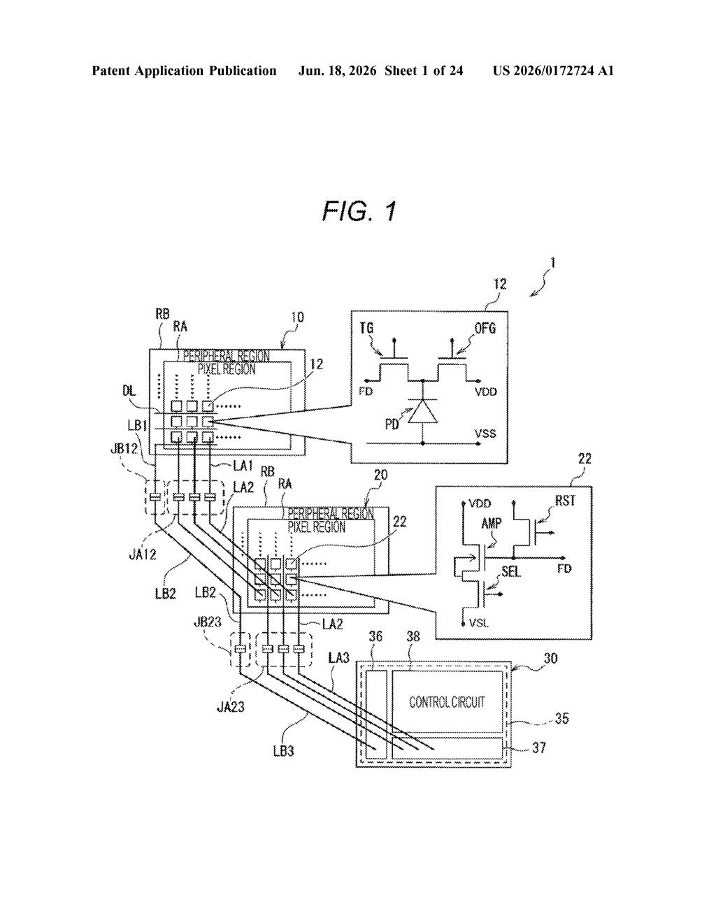
- Publication number
- US 2026/0172724 A1(US20260172724A1)
- Applicant
- SONY SEMICONDUCTOR SOLUTIONS CORPORATION
- Filed · Published
- Feb 11, 2026 · Jun 18, 2026
- Inventors
- Kyosuke YAMADA, Atsuhiko YAMAMOTO, Takashi MACHIDA, Hideo KIDO, Ryo FUKUI, Yu SHIIHARA
- Status when we published
- Waiting for an examiner
- Document
- 13 claims
- US classification
- 250/208.1
- Parent application
- Continuation of 18/001,299 (filed Dec 9, 2022)(18001299)
What Sony's stacked image sensor design actually does
Imagine your camera's sensor as a tiny apartment building. Light hits the top floor (the sensor pixels), and the electrical signal travels downstairs to a processing floor that reads and amplifies it. The problem is when the downstairs neighbors are noisy — other circuits on the same floor can create electrical interference that degrades the final image.
Sony's approach is essentially to build a firewall into the chip itself. The amplifier transistor — the circuit that boosts the faint electrical signal from each pixel — gets its own physically isolated zone. A trench cut through the thickness of the semiconductor substrate separates it from everything else nearby.
This matters because the two halves of the chip (the pixel layer and the readout layer) are bonded directly together at the electrode level, which is already an efficient design. Adding isolation on top of that is Sony trying to make sure that efficiency doesn't come at the cost of image quality.
How the through-region isolates the amplifier transistor
The patent describes a stacked image sensor made of two bonded substrate layers. The first substrate carries the sensor pixels — the light-absorbing elements that convert photons into electrical charge via photoelectric conversion. The second substrate, bonded face-to-face with the first, carries the readout circuit that turns that charge into a usable pixel signal.
The two layers connect through directly bonded electrode pairs — no solder bumps, no wires, just metal-to-metal contact at the interface. That direct bonding (sometimes called hybrid bonding in the industry) keeps the signal path short and reduces resistance.
The key innovation is inside the second semiconductor substrate. It is divided into three distinct zones:
- First element region — where the amplification transistor lives (this transistor boosts the faint charge signal from each pixel into a readable voltage)
- Second element region — where other circuit elements sit
- Through region — a trench or gap that runs completely through the substrate's thickness, physically separating the first and second element regions
By running an isolation barrier all the way through the chip rather than just along the surface, Sony aims to prevent electrical crosstalk (unwanted signal leakage between neighboring components) from reaching the amplification transistor and distorting the output.
What this means for future Sony camera and phone sensors
For consumer cameras and smartphone sensors, noise and crosstalk are persistent enemies of image quality, especially in low-light conditions where amplification is pushed hardest. If the amplifier transistor picks up interference from adjacent circuits, the result shows up as fixed-pattern noise or degraded dynamic range — problems that software processing can only partially fix.
Sony Semiconductor Solutions supplies image sensors to a large share of the global smartphone market, including Apple's iPhone line. A structural improvement that preserves signal integrity at the chip level — rather than compensating for it in software — could quietly raise the baseline quality of sensors that end up in hundreds of millions of devices.
Source: US 2026/0172724 A1 at the USPTO (PDF). Full patent text and figures are in the official publication.
Get our take in your Top Stories
Liked this breakdown? Add Patentlyze as a preferred source on Google, and our plain-English take shows up more often in your Top Stories the next time Sony patent news breaks.
Add Patentlyze on Google
One click.
There are more where this came from
We read every patent application Big Tech publishes and send you the ones worth knowing. Plain English, free, every week.
More from Sony
All 707 Sony patents →

More in Chip
All 645 Chip patents →
Qualcomm
Qualcomm Patents a Chip That Checks Its Own Safety Systems While Running
OpenAI
OpenAI Patents a Chip That Runs AI Calculations Forward and Backward Without Interruption

Qualcomm
Qualcomm Patents a Chip That Stores Data and Calculates It Simultaneously

Intel