
Samsung Patents a Built-In Interference Barrier for Multi-Antenna Radio Modules
Pack too many antennas onto a single circuit board and they start talking over each other, degrading the signal for everyone connected. Samsung's latest patent addresses that problem by placing a conductive divider directly between antenna elements on the same substrate layer.
What Samsung's antenna-separation trick actually does
A cell tower's radio unit sits in a weatherproof box handling thousands of wireless connections at once. Most people never see it, but the engineers who design the hardware inside face a recurring headache: the more antennas you cram onto a single board, the more those antennas interfere with one another.
Samsung's patent describes a radio module where a conductive member (essentially a strip of electrically active material) is placed between two antenna elements on the same layer of a circuit board. Think of it as a thin wall between neighbors who are too loud. The surrounding circuit board is built from multiple stacked layers, and the conductive member runs across those layers to help channel and isolate the signals each antenna is trying to send or receive.
The design targets radio unit (RU) modules, the hardware blocks used in modern 5G base stations and similar telecom equipment. Better antenna isolation in a compact module means cleaner signals, which can translate to more reliable connections for the people those towers serve.
… a conductivity member, and wherein at least a portion of the conductivity member is disposed between the first antenna element and the second antenna element that are on the at least one layer of the substrate.
Translation: A physical barrier sits right between two antennas to block unwanted signal interference.
How the conductive member sits between two antenna elements
The patent describes a radio unit (RU) module, a self-contained hardware assembly used in 5G and next-generation wireless infrastructure.
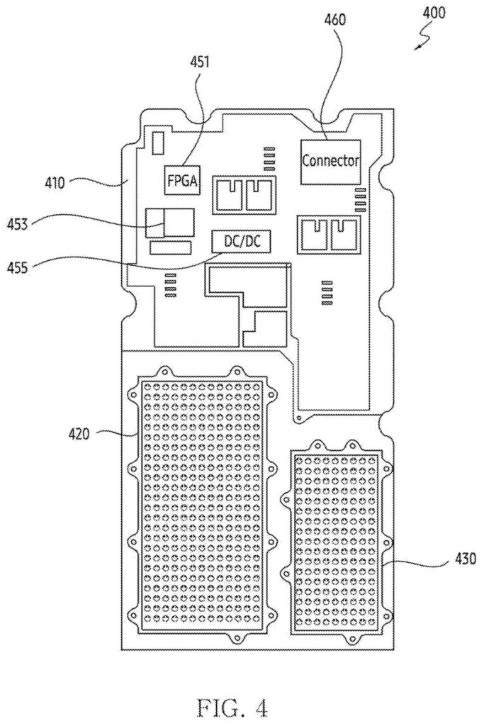
At its core, the design stacks two circuit boards. A first substrate carries a radio frequency integrated circuit (RFIC) on one face (the chip that actually processes radio signals). A second substrate, made of multiple bonded layers, attaches to the opposite face of the first board. The antenna elements sit on specific layers within that second substrate.
The key claim is the placement of a conductivity member: at least part of it must sit between the first and second antenna elements on the same layer. That positioning creates a localized electromagnetic barrier (a physical structure that changes how electric fields behave in the space between the two antennas), reducing the amount of signal energy that bleeds from one antenna into its neighbor. The member extends across multiple layers of the second substrate, giving it depth as well as width.
The arrangement allows:
- Multiple antenna elements packed closely together on a shared board
- A built-in isolation structure that does not require extra external shielding components
- The RFIC and antennas to share a compact, vertically integrated module
The plurality of conductivity members may be disposed across the plurality of second layers of the second substrate.
Translation: Multiple shielding walls are built directly into the circuit board layers.
What this means for 5G base stations and dense radio gear
In 5G base stations, antenna modules need to fit more and more antenna elements into tighter spaces to support features like beamforming (where the radio focuses its signal toward specific devices rather than broadcasting in all directions). Interference between nearby antennas is one of the main things that limits how tightly you can pack them. A solution built into the substrate itself, rather than bolted on as an aftershield, could make those modules smaller and cheaper to produce.
For everyday users, the downstream effect would be the kind of 5G performance that actually matches the spec sheet: more consistent throughput in crowded areas, fewer dropped connections when a tower is serving a lot of devices at once. The practical payoff depends on how well the design scales to real production hardware, but the problem it targets is real and pressing for any carrier building out dense 5G networks.
Samsung's 81st filing we've tracked since May in our 5G and network work sits alongside one on a hidden antenna slot and one on permission-based 5G access.
Slipping a physical divider between neighboring antennas on the same board trades away space and forgives almost nothing in assembly. If that barrier lands even slightly off-center during manufacturing, it can create the very interference it was designed to prevent, just in a different direction.
For a base station meant to sit outdoors for years, the bet still reads as sensible. A passive metal wall has far fewer ways to fail over time than any active electronic component, and the hardware is expensive enough that a little extra material costs almost nothing by comparison.
The real gap is that the patent describes a shape, not a measured result. Without numbers showing how much actual interference gets blocked, this is a structurally plausible answer to a known problem, and whether it works well enough in practice remains an open question.
There are more where this came from
We read every patent application Big Tech publishes and send you the ones worth knowing. Plain English, free, every week.
The drawings
28 drawing sheets from US 2026/0291055 A1 · click any drawing to enlarge


Want this weekly breakdown for a company we don't cover? Patentlyze Pro →
Be the first to weigh in