
Samsung Patents a Chip That Moves Data With Light Instead of Electrical Signals
Samsung has filed a patent for a processor package that sends and receives data using pulses of light rather than electrical signals, with the optical hardware built directly into the same package as the chip and memory.
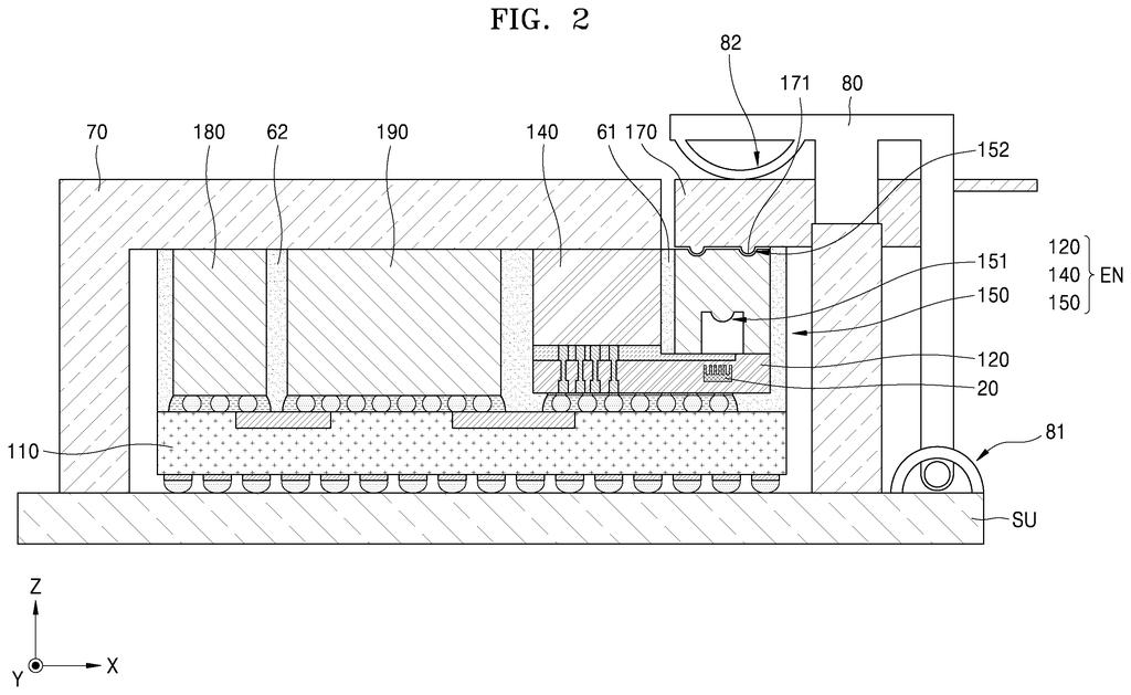
How Samsung wants to move data using light inside a chip
A data center server pushes enormous amounts of information between chips every second. Today that data travels as electricity through copper wires, and electricity has limits: it generates heat, slows down over distance, and consumes a lot of power. Light signals don't have those same problems.
Samsung's patent describes a chip package that bakes an optical engine directly into the hardware alongside the processor and memory. That optical engine converts electrical signals into light and back again, and it connects to fiber-optic cables through a precision alignment groove. Think of the groove as a tiny slot that holds the fiber cables in exactly the right position so no light is lost.
For you as an end user, the direct benefit is indirect but real: servers that move data faster and cooler could mean quicker responses from cloud apps, AI services, and anything else running in a data center. This isn't about your phone; it's about the machines that power the services on your phone.
… an optical engine on the interposer, wherein the optical engine comprises: a photonic integrated circuit (PIC) chip comprising circuit elements configured for photoelectric conversion …
Translation: The chip uses light-based components to convert electrical signals into optical signals.
How the groove structure lines up fiber optics to the chip
The patent describes a processor package built on a component called an interposer (a thin substrate that connects multiple chips together, like a circuit-board layer dedicated to chip-to-chip wiring). Sitting on that interposer are three main components: a processor, memory, and an optical engine.
The optical engine contains a photonic integrated circuit (PIC) chip, which is a chip designed to handle light the way a regular chip handles electricity. It includes components for photoelectric conversion, meaning it can turn electrical signals into light pulses and light pulses back into electrical signals. This is the same basic idea as fiber-optic internet, but miniaturized to fit on a chip package.
On top of the PIC chip sits a coupling structure that gives light a physical path in and out of the package. The key detail is a groove structure on the upper surface of that coupling structure. The groove is designed to mechanically align a fiber array unit (FAU), which is essentially a ribbon of multiple fiber-optic cables held in a precise arrangement.
- The groove removes the need for active electronic alignment during manufacturing, reducing assembly complexity.
- Keeping everything on one interposer shortens the electrical path between processor, memory, and the optical interface.
- The PIC chip handles signal conversion locally, so data can leave the package as light immediately.
… at least one groove structure configured for alignment with a fiber array unit (FAU).
Translation: Specialized physical grooves help align the microscopic optical pathways with external fiber optic cables.
What light-based chip links mean for data centers
Electrical connections inside data center equipment are hitting physical limits. Moving more data means more copper traces, more heat, and more power draw. Light-based interconnects have long promised a way out of that constraint, but they have historically been separate, external modules bolted onto servers rather than integrated with the processor itself.
A package that puts the optical engine on the same interposer as the processor and memory collapses that distance dramatically. For AI training clusters and high-performance computing racks, where chips need to share enormous datasets with each other at speed, tighter optical integration could reduce the bottleneck between compute and communication. Samsung has been filing around chip-level optical integration for some time, and this patent adds a specific, manufacturable alignment approach to that body of work.
Samsung's 59th filing we've tracked in the AI chip wars since June adds to a pattern started by one on avoiding memory drain and one that reroutes overloaded memory chips.
Samsung's patent describes a small groove carved into a chip that guides fiber-optic cables into exact alignment, solving a fiddly physical problem that stands between today's electronics and computers that move data using light instead of electricity.
The catch is that this is a hardware invention, meaning every physical piece has to exist and cooperate before anything ships. The groove needs cables manufactured to match it, chips that actually convert light reliably, and factories capable of assembling all of it cheaply enough to matter.
The specificity of the groove design suggests real prototypes have been built and handled, which is a meaningful step forward. But between a working prototype and a product in a data center lies a chain of supply agreements, manufacturing decisions, and cost negotiations that a patent cannot resolve on its own.
There are more where this came from
We read every patent application Big Tech publishes and send you the ones worth knowing. Plain English, free, every week.
The drawings
12 drawing sheets from US 2026/0299227 A1 · click any drawing to enlarge


Want this weekly breakdown for a company we don't cover? Patentlyze Pro →
Be the first to weigh in