
AMD Files Patent for AI Chips With a Built-In Spare for Manufacturing Flaws
Today, one microscopic flaw can send an entire AI chip to the scrap bin. A patent application from AMD's Xilinx unit gives the chip a spare column of processing blocks, so a single defect doesn't doom it.
What AMD's spare-column AI chip actually does
Ever bought a dozen eggs and found one cracked? You skip that egg and use the other eleven. Computer chips are less forgiving: one microscopic flaw in the wrong spot can mean the whole chip gets thrown away.
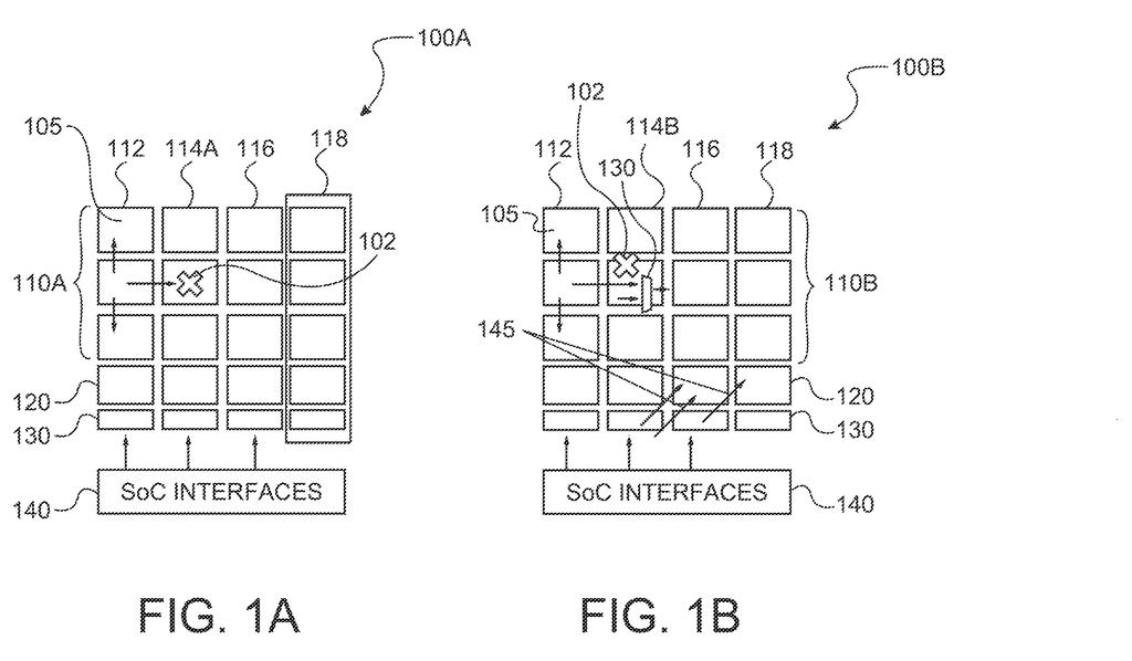
This patent application, filed under AMD's Xilinx unit, tackles that problem for AI chips. It adds an extra spare column of processing blocks that sits unused until it's needed. When the chip powers on, it checks itself. If one column is broken, built-in switches steer the work around it and onto the spare.
The software running on top never notices. It sees a normal chip, as if nothing went wrong. A chip built with four columns could be sold as a working three-column chip, and a flaw that would have meant the trash becomes a non-event.
… a bypass circuit configured to detect a defective column of the array of tiles and re-route at least signals, operations, memory interfaces, or data flows from the defective column to the redundant column.
Translation: A built-in system spots broken parts and automatically redirects work to the backup lanes.
How the chip swaps a broken column at boot
The filing describes an AI engine array: a grid of small processing tiles arranged in rows and columns, each with its own compute unit, memory and connections to its neighbors. One column of that grid is designated a redundant column, an identical spare that stays idle (and saves power) on a healthy chip.
A bypass circuit watches over the array. The claims break it into a few parts:
- Defect detection circuitry (sensors or diagnostic units) that monitors chip components and flags a problem.
- Multiplexers and switches (electronic traffic switches that pick which path a signal takes) that re-route signals, operations, memory connections and data flows.
- Control logic that makes the re-routing decisions without a person stepping in.
The description says the swap happens at boot time. The chip runs a built-in self-test, or reads a permanent fuse setting programmed during factory testing, to learn which column is bad. It then isolates that column and remaps the work to the spare. Memory addresses are shifted so software still sees one continuous block of memory.
The filing also describes options: a user can set how tall the replaced column is, with a row-skipping method for partial cases, and an array can carry several spare columns. Claims cover the engine itself, a method, and a full system-on-chip (a chip that packs many components together) containing these engines.
… defect detection circuitry configured to monitor chip components and flag defects, multiplexers and switches to re-route the signals, operations, or data flows from the defective column to the redundant column, and control logic for orchestrating re-routing decisions.
Translation: Specialized hardware monitors the chip and uses switches to route around any broken manufacturing flaws.
Why spare parts could cut AI chip waste
Chips come off the factory line with flaws, and the bigger and denser an AI chip gets, the more likely a flaw becomes. Every chip that gets scrapped is a cost the maker has to recover somewhere. A spare column is a way to save chips that would otherwise be lost, which could help keep your AI hardware's price down. The filing itself ties the idea to higher manufacturing yield, lower production costs and less waste.
It also hints at a sales trick: build a four-column array and sell it as a reliable three-column part. The filing says this gives makers high-reliability hardware at minimal added cost. Remember that this is a patent application, not a product. The filing names no specific chip, and the boot-time design means it won't help with failures that show up later in use.
AMD's 44th filing we've tracked in the AI chip wars since May builds on the one-step AI math patent and the memory traffic cut.
The cost of this design is easy to name: you build a whole extra column that does nothing on a healthy chip. That is silicon you pay for and never use, and it only pays off if flaws are common enough to justify the spare.
The filing is upfront about other limits. The swap happens only when the chip starts up, so a column that fails weeks later in the field is not rescued. One spare covers one bad column, and a second flaw in a different column leaves the chip as scrap. Adding more spares fixes that but costs more chip area, more power and more wiring to manage.
Even so, the trade reads as worth it. AI chips keep growing, which makes flaws likelier, and a spare column is a modest price against throwing out an entire expensive chip. It is sensible insurance, and the boot-time-only limit keeps the added complexity low.
Get our take in your Top Stories
Liked this breakdown? Add Patentlyze as a preferred source on Google, and our plain-English take shows up more often in your Top Stories the next time AMD patent news breaks.
There are more where this came from
We read every patent application Big Tech publishes and send you the ones worth knowing. Plain English, free, every week.
The drawings
5 drawing sheets from US 2026/0311794 A1 · click any drawing to enlarge


Want this weekly breakdown for a company we don't cover? Patentlyze Pro →
Be the first to weigh in