
Sony Files Patent for a Camera Sensor That Handles Both Dim Rooms and Bright Sun
A camera sensor that captures every pixel at the same instant has a noise problem, and Sony's fix is to let each pixel read light two ways, one for dim scenes and one for blinding ones, with a different-sized storage spot for each.
What Sony's two-gear camera pixel actually does
A phone camera points at a dim restaurant table, then swings toward a window full of afternoon sun. Those two scenes ask very different things of the sensor, and a sensor tuned for one tends to struggle with the other.
Sony's patent application is about a type of sensor that exposes every pixel at the same moment. These sensors hold each pixel's reading in a tiny electrical storage cell until it can be sent out, and that holding step adds noise, which shows up as grain. The earlier design Sony points to couldn't change how strongly it turns light into a signal, so dim scenes came out too weak and bright ones could clip.
Sony's version lets each pixel read light at two strengths, one for dim scenes and one for bright ones, and gives every reading its own storage cell. The cell for the sensitive, dim-light reading is made larger, since that is where noise does the most damage. In practice, your photos could hold on to both shadows and highlights.
a high capacitive element whose capacitance value is higher than a predetermined value, and a low capacitive element whose capacitance value is lower than the predetermined value …
Translation: The sensor uses different circuit parts to handle bright light and dark shadows separately.
How Sony sizes the storage cells for each gear
The core is a pixel that can turn captured light into a voltage at more than one conversion efficiency (how much voltage you get for each bit of light collected). High efficiency suits dim scenes. Low efficiency suits bright ones, where a pixel would otherwise fill up and clip.
After the exposure ends, the pixel sends out its readings one after another: a reset level and a signal level at high efficiency, then the same pair at low efficiency. Each reading is parked in its own capacitive element (a tiny electrical storage cell). All the cells share one connection on the input side, and a selection circuit (a set of switches) links just one at a time to the readout. The chip then subtracts the reset level from the signal level to cancel out offsets, and can choose the high or low reading for a whole frame or pixel by pixel, depending on brightness.
The claimed twist is that the cells come in different sizes. The high-efficiency reading goes into a bigger cell, because a larger cell cuts kTC noise (random electrical fuzz created when a voltage is sampled), and that fuzz matters most at high efficiency. The filing describes several ways to build the bigger cell:
- Give it a larger area.
- Use a denser capacitor material in the same footprint.
- Wire several identical small cells together so they act as one.
A separate independent claim covers another route: two extra capacitors of different sizes, attached to the pixel's charge-collecting spot through two switches, so the pixel can step through several gain levels.
In a solid-state imaging element that performs exposure in all pixels at the same time, image quality is improved.
Translation: Exposing every pixel simultaneously helps the camera produce much clearer pictures.
What this means for low-light and bright photos
If you shoot in a dim room one minute and bright sun the next, a sensor that adapts for each pixel could keep more detail at both ends without piling on grain. The filing says the sensor would go into a digital camera or a device with a camera, such as a smartphone or personal computer, and it also describes a vehicle application.
For Sony, which designs image sensors through its semiconductor unit, the value is in fixing a known weakness of this sensor type: earlier designs could not change their gain. The filing continues an earlier application first filed in Japan in October 2021. A published application is a request for protection, not a product announcement.
Sony's 97th filing in Display patents we cover since May follows one on shrinking panel circuits and one on flagging image regions.
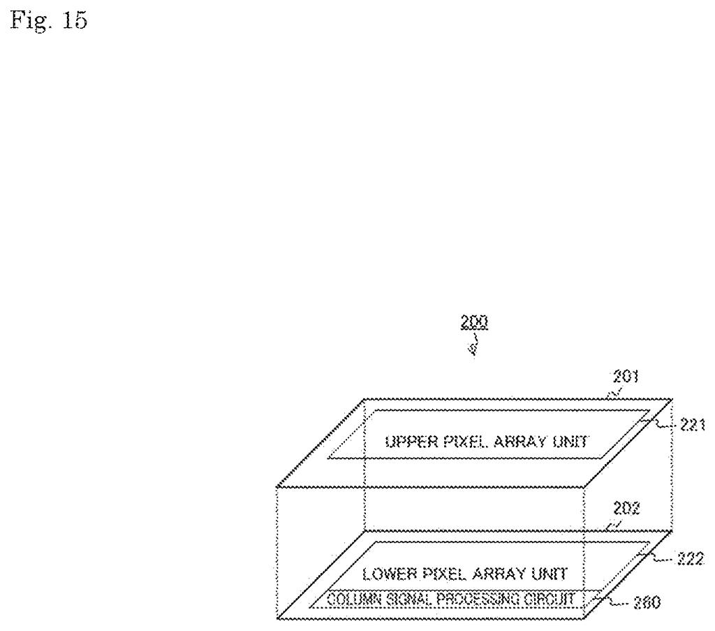
Every extra storage cell inside a pixel costs room, and pixels are already tiny. Sony's design asks each one to carry four holding spots instead of two, plus the switches to pick between them, and the biggest of those spots has to be even bigger.
The filing is open about that squeeze. It spreads the parts across stacked chips, packs more storage into the same footprint, or wires several small identical cells together so they act as one large one. Each route adds manufacturing complexity, and the description says one variant is partly meant to hold down development costs.
The trade looks sensible anyway. Spending space only where noise hurts most, on the sensitive dim-light reading, is a targeted choice, and the payoff is a camera that no longer has to pick between good shadows and unclipped highlights. The open risk is that a sensor this crowded could force larger pixels or lower resolution, and the document gives no numbers on that.
Get our take in your Top Stories
Liked this breakdown? Add Patentlyze as a preferred source on Google, and our plain-English take shows up more often in your Top Stories the next time Sony patent news breaks.
There are more where this came from
We read every patent application Big Tech publishes and send you the ones worth knowing. Plain English, free, every week.
The drawings
79 drawing sheets from US 2026/0352974 A1 · click any drawing to enlarge


Show the other 52 sheets


Sheets 61 to 79 are in the full USPTO filing.
Want this weekly breakdown for a company we don't cover? Patentlyze Pro →
Be the first to weigh in