
Intel Patents a Processor Instruction for Faster Parallel Matrix Math
Matrix multiplication is the core arithmetic behind almost every AI model, and Intel is patenting a way to make processors handle it in bigger, parallel bites rather than one piece at a time.
What Intel's block-wise matrix math actually does
Every time an AI model generates a word, produces an image, or recognizes your face, a processor somewhere is grinding through enormous grids of numbers called matrices. Multiplying those grids together is the single most repeated operation in AI computing, and doing it fast is the difference between a model that responds in a second and one that makes you wait.
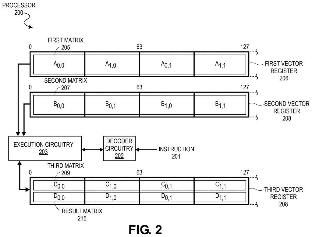
What Intel is patenting here is a new processor instruction that splits large matrices into smaller blocks, stores each block in its own memory slot inside the chip (called a vector register), and then multiplies all those blocks at the same time in a single coordinated step. Instead of your chip chewing through one chunk at a time, it tackles the whole grid in one coordinated move.
For you as an end user, this kind of chip-level efficiency is what makes AI features on laptops and phones feel fast rather than sluggish. It's invisible plumbing, but the kind that decides whether a product feels snappy or frustrating.
… a decoder to decode an instance of a multi-register cross-product matrix multiply instruction having fields to indicate the first and second source matrices and the result matrix …
Translation: The chip includes a decoder that reads the special matrix multiplication instruction and identifies the input and output data.
How the cross-product instruction splits and multiplies matrices
The patent describes a new type of processor instruction called a multi-register cross-product matrix multiply instruction. An instruction, in chip terms, is a single command the processor knows how to execute natively at the hardware level.
Here is what the system does step by step:
- Splitting: Two large source matrices (grids of numbers) are each divided into smaller pieces called sub-matrices, and each piece is loaded into its own vector register (a fast, on-chip memory slot designed to hold data for parallel processing).
- Instruction decoding: A decoder inside the chip reads the new instruction and identifies which registers hold which sub-matrices and where to write the results.
- Parallel multiplication: The chip's execution circuitry multiplies corresponding sub-matrix pairs simultaneously across all the register sets, generating a third set of sub-matrices that together form the result matrix.
The key design choice is the cross-product nature of the operation. Rather than requiring software to loop through each block manually, the single instruction triggers the whole block-wise multiplication in one hardware pass. This reduces the number of instructions the processor has to fetch and decode, which is often the hidden bottleneck (called instruction overhead) in high-throughput computing.
The patent covers the decoder logic, the register layout, and the execution circuitry together, meaning Intel is protecting the whole pipeline from instruction entry to result output.
… execution circuitry to generate each sub-matrix of the third plurality of sub-matrices in a corresponding vector register of the third plurality of vector registers by multiplying a sub-matrix in a corresponding vector register of the first plurality of vector registers and a sub-matrix in a corresponding vector register of the second plurality of vector registers …
Translation: The hardware calculates the final matrix blocks by multiplying the corresponding source matrix blocks together.
What this means for AI chips and workload speed
Matrix multiplication sits at the center of neural network inference and training, the two main workloads driving demand for AI chips right now. Any processor improvement that reduces how many steps a chip takes to complete that math translates directly into lower power consumption and higher throughput, which matters whether the chip is inside a data center server or a laptop running a local AI model.
Intel has been competing hard with Nvidia and AMD for AI workload share, and architectural patents like this one signal where its hardware teams are placing their bets at the instruction-set level, the deepest layer of chip design. Chip-architecture filings from Intel are a steady part of the Big Tech patent news stream that tracks how CPU makers are rebuilding their cores around AI math.
That makes this Intel's 31st filing we've tracked since May in the AI chip wars watchlist, joining one on memory spying defense and one on mid-instruction bookmarking.
Matrix multiplication sits at the heart of nearly every AI calculation, from recognizing a face in a photo to generating a sentence. Processors today handle it by repeating small steps in a loop, spending a surprising share of their time on bookkeeping rather than actual math. Collapsing those repeated steps into a single instruction the chip understands natively is a direct attack on that waste.
Less overhead per calculation means more useful work per second, which compounds quickly when a data center runs millions of these operations per minute. The problem is large enough that even modest efficiency gains translate into meaningful reductions in cost and energy at scale.
A patent this specific, targeting a named formulation of the operation, suggests Intel is designing this into real silicon rather than filing speculatively.
Get our take in your Top Stories
Liked this breakdown? Add Patentlyze as a preferred source on Google, and our plain-English take shows up more often in your Top Stories the next time Intel patent news breaks.
There are more where this came from
We read every patent application Big Tech publishes and send you the ones worth knowing. Plain English, free, every week.
The drawings
31 drawing sheets from US 2026/0252663 A1 · click any drawing to enlarge


Want this weekly breakdown for a company we don't cover? Patentlyze Pro →
Be the first to weigh in