
Google Files Patent for an AI Chip Broken Into Sections With Separate Memory Lanes
Google's chip design treats AI math like a team sport: a grid of small tiles, one road for passing notes to neighbors, and a separate loop for calling out to the whole room.
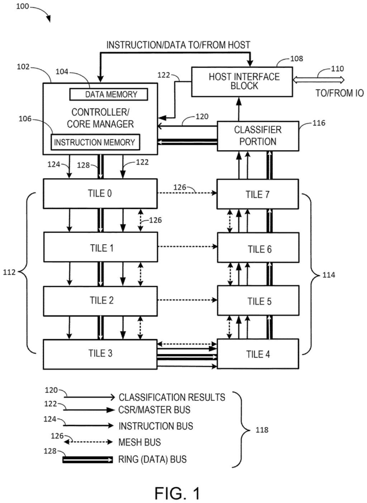
What Google's tiled AI chip actually does
Ever organized a group project where everyone needs the same instructions, but each person also has to pass partial results to the person beside them? Push all of that through one shared channel and the room becomes a traffic jam.
Google's patent application tackles that problem inside AI chips. Instead of one giant processor, the chip is a grid of small tiles. Each tile has two kinds of memory: a narrow one for the data it is working on right now, and a wider one for the model's stored numbers (called weights).
The tiles then talk over two separate roads. One links each tile to its neighbors for handing along in-progress data. The other is a loop around the whole chip that broadcasts shared numbers to whichever tiles need them, so a single message can reach many tiles at once.
… a mesh bus providing a first data communications path that couples each compute tile to one or more compute tiles adjacent to the compute tile, wherein the mesh bus is configured to transport input activation quantities between narrow memory units in adjacent compute tiles …
Translation: A local network moves working data directly between neighboring processing sections.
How the ring loop tells tiles who gets data
The claims describe a hardware system made of many compute tiles. Each tile holds a narrow memory (a small-width store for the data flowing through a neural network layer, called input activations) and a wide memory (a larger-width store for the weights, the learned numbers those inputs get multiplied by).
Two separate connections tie the tiles together. The mesh bus links each tile to its adjacent tiles and moves input activations between their narrow memories. The ring bus is a distinct loop through all the tiles that multicasts (sends one copy to many receivers) payload data, such as activations and weights, into the wide memories.
The ring has some careful traffic rules:
- A bitmap header (a row of on/off bits) marks which tiles should keep the data. Each tile clears its own bit after taking the payload, and forwarding stops once no bits are left.
- Only one tile sends on the ring at a time. A controller counts each write with a sync flag count and blocks other tiles until the expected number of data segments has gone out.
- Separate, non-overlapping groups of tiles can each have their own sender at once.
Inside each tile, a tensor traversal unit generates memory addresses to walk through multi-dimensional data using nested loops. An array of multiply-accumulate cells then does the math, multiplying an input from the narrow memory by a weight from the wide memory.
… at least one cell comprising at least one multiply accumulate (“MAC”) operator that receives parameters from the second memory bank and performs computations …
Translation: Specialized math circuits pull stored settings from memory to run calculations.
Why moving data matters for Google's AI chips
Behind any AI feature you use, a chip is shuffling enormous piles of numbers, and much of the design work goes into getting the right numbers to the right place at the right time. This layout gives each tile its own storage and gives data two dedicated routes, so the multiplying units should spend less time waiting. The description also says one instruction can drive a deeply nested loop of math, which cuts instruction traffic.
The filing names no product and gives no speed figures, so treat it as a look at how Google organizes this kind of hardware. It continues an application first filed in 2016, and the claims here center on the two-road layout. If it pays off, you would see it as cheaper, cooler AI processing, which eventually means faster or less costly AI features.
This is the 24th Google filing we've tracked since July in our AI chip wars, following voice assistant priority and add-before-multiply chip idea.
Every choice in this design buys speed by giving something up. Only one tile can broadcast on the loop at a time, so the others wait their turn while a controller counts writes. Neighbor-only links on the mesh mean data headed far across the chip has to hop through tiles in the middle.
In return, no single shared channel has to carry everything, and each road suits its job: the loop is as wide as the big memory it feeds. Two sets of wiring cost chip space and add coordination rules designers must get exactly right, since the description warns that overlapping groups can corrupt each other's data.
For a chip whose whole purpose is keeping math units fed, the trade reads as worth it. The filing gives no performance numbers, though, so how much it pays off stays an open question.
Get our take in your Top Stories
Liked this breakdown? Add Patentlyze as a preferred source on Google, and our plain-English take shows up more often in your Top Stories the next time Google patent news breaks.
There are more where this came from
We read every patent application Big Tech publishes and send you the ones worth knowing. Plain English, free, every week.
The drawings
6 drawing sheets from US 2026/0339665 A1 · click any drawing to enlarge


Want this weekly breakdown for a company we don't cover? Patentlyze Pro →
Be the first to weigh in