
Sony Patents a Way to Wake Up Chips Using the Data Line They're Already On
Sony has filed a patent for a method that lets a controller chip tell connected chips to come out of their startup freeze, without needing a separate physical wire dedicated to that job.
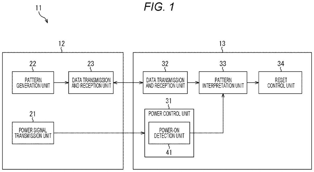
How Sony's reset signal travels on an existing wire
A security camera stares at an empty hallway all night. Inside it, a handful of chips are waiting to receive instructions before they do anything. Right now, one common way to give those chips the "go ahead" signal is to run a dedicated wire from the main controller to each chip. Sony's patent describes cutting out that extra wire entirely.
Instead of a separate line, the controller sends a specific coded sequence (a "reset pattern") down the same data wire the chips already share. A chip that receives this sequence recognizes it as the signal to stop waiting and start working. The chip has a small piece of logic whose only job is to watch for that specific pattern and trigger the startup process when it arrives.
For consumer electronics with many chips crammed into a tight space, fewer wires means simpler circuit boards, lower costs, and potentially fewer things that can go wrong during manufacturing.
a pattern interpretation unit that determines whether or not a target reset pattern has been received, the target reset pattern being transmitted from the controller device through a data communication line and instructing first reset release after the target device is powered on …
Translation: A special detector watches the data line to spot a specific wakeup signal sent after power on.
How the target device reads and acts on the reset pattern
The patent describes a communication system made up of two types of participants: a controller device (the chip in charge) and one or more target devices (chips that follow orders). All of them share a common data communication line, similar to a party line where everyone can hear what is sent.
After a target device powers on, it sits in a reset state (a frozen condition where it waits before doing anything). Normally, releasing that freeze requires either a dedicated reset wire or a more complex initialization sequence. This patent skips that by encoding a special bit pattern directly into the data stream.
Each target device includes two key components:
- A pattern interpretation unit that continuously monitors the data line and checks whether the incoming signal matches the pre-agreed "target reset pattern."
- A reset control unit that, once a match is confirmed, releases the reset state so the chip can begin normal operation.
The system is described as compatible with the I3C specification (a modern short-range chip-to-chip communication standard used widely in smartphones, cameras, and sensors). Because the reset pattern travels on the existing data line, no extra physical connection is required.
… a reset control unit that performs control to release a reset state of the target device in a case where the target reset pattern is determined to have been received.
Translation: Once the chip recognizes that specific signal, it wakes up and starts operating normally.
What this means for device startup in compact electronics
For engineers designing compact devices like phones, wearables, or camera modules, every trace on a circuit board costs space and money. Eliminating a dedicated reset line is a small but real saving, especially when dozens of chips are involved. It also removes one category of hardware fault: a reset wire that corrodes, breaks, or is simply mis-routed during assembly.
For end users, the payoff is indirect. You would notice it as a device that starts up more reliably, or as a product that is thinner or cheaper because the internal board is simpler. Sony has been filing around chip-to-chip communication since at least 2024, reflecting the company's deep investment in the sensor and semiconductor hardware that sits inside cameras and mobile devices.
Sony's eighth filing since July in our AI chip wars watchlist, following one that cuts chip memory instantly and one linking display chips, adds another piece to how the company is rethinking chip design.
A chip inside your phone that fails to wake up correctly after powering on can cause the whole device to freeze, reboot unexpectedly, or simply refuse to start. Sony's patent addresses exactly that moment, encoding a startup instruction directly into an existing data connection rather than requiring a dedicated physical wire to do the job.
Fewer wires between chips means fewer things to go wrong during manufacturing. That translates to devices that boot reliably, behave consistently across their lifetime, and are less likely to arrive with subtle hardware faults already baked in.
You will never see this mechanism at work, and that invisibility is precisely what success looks like here. The engineers building your next device will have one less failure point to worry about, and you will simply have a phone that turns on when you press the button.
There are more where this came from
We read every patent application Big Tech publishes and send you the ones worth knowing. Plain English, free, every week.
The drawings
14 drawing sheets from US 2026/0288216 A1 · click any drawing to enlarge


Want this weekly breakdown for a company we don't cover? Patentlyze Pro →
Be the first to weigh in