
Samsung
Samsung · Chip · Filed Mar 23, 2026 · USPTO published Nov 12, 2026 · This week's release
Samsung Patents a Memory Chip Design That Does AI Math Where Data Is Stored
Samsung has drawn up a memory cell that does the math itself, so an AI chip doesn't have to keep hauling numbers back and forth. It manages this with just six transistors.
- Publication number
- US 2026/0360400 A1(US20260360400A1)
- Applicant
- SAMSUNG ELECTRONICS CO., LTD.
- Filed · Published
- Mar 23, 2026 · Nov 12, 2026
- Inventors
- Changseung LEE, Jaechul PARK, Hyeongseok JANG, Sungchan KANG, Seunggeol NAM, Jungyeop OH
- Status when we published
- Waiting for an examiner
- Document
- 20 claims
- US classification
- 365/189.011
What Samsung's math-doing memory cell does
A phone running an AI feature spends a surprising amount of energy just shuffling numbers between its memory and its calculator chip. Your battery pays for every one of those trips.
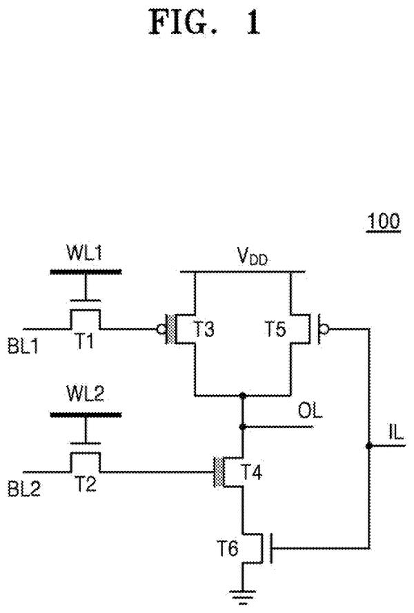
Samsung's patent application describes a tiny circuit that skips the trip. Each cell holds a stored number and also does the arithmetic on it, right where it sits. It uses six transistors (the microscopic switches inside chips), and two of them are special ferroelectric switches that remember their setting even with the power off.
An AI model's learned numbers rarely change, so they can stay put in the cells while fresh data flows past. The filing says this could shrink the circuit and cut the power a chip burns while it is just waiting.
… wherein the third transistor and the fourth transistor are programmable transistors
Translation: Two special transistors can be reprogrammed to handle the chip's processing tasks.
How the six-transistor cell stores and computes
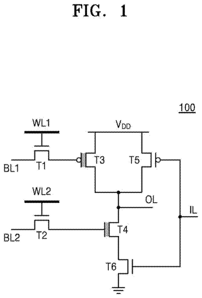
Claim 1 covers a bitcell, the smallest unit of memory, built from six transistors plus a set of control wires: two word lines, two bit lines, an input line and an output line. Two of the transistors are programmable, meaning their threshold voltage (the voltage at which the switch flips on) can be set to stand for a 0 or a 1. The claims name a ferroelectric transistor (FeFET), a type that keeps its setting without power.
Writing happens in two steps. First, a voltage matching the bit goes onto one bit line while certain switches are on and others off. Then the opposite (complementary) voltage goes onto the second bit line. Both programmable transistors end up holding the same bit.
Computing is a separate step. Medium-strength read voltages go onto both bit lines, and a voltage representing a second bit goes onto the input line. The output line then shows the result. The description says the four transistors involved form a NAND gate, a basic logic building block that outputs 0 only when both inputs are 1. In AI terms, the stored bit is a weight and the incoming bit is data.
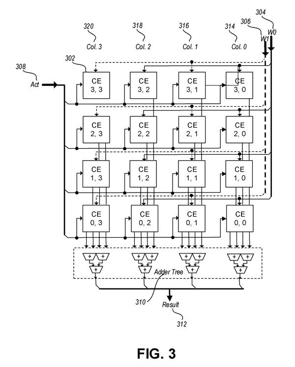
The filing also covers arrays of cells. One example is a 4×4 grid in which columns compute in parallel, an adder tree circuit sums the outputs, and an accumulator produces the final total. An optional seventh transistor is also described.
What this could mean for AI on your devices
The practical pitch is AI that costs less power. The filing says storing data in these nonvolatile switches could greatly cut the power a chip draws while idle, and that on-chip memory could hold more in the same area. Both matter in anything running on a battery.
The filing lists smartphones, smart TVs, robots, medical devices and other connected gadgets as places this could go. It is still a patent application, and it gives no measured results or product plans. Whether anyone can build these cells cheaply at scale is a question the document does not answer.
Samsung's 65th filing we've tracked since June in our AI chip wars watchlist builds on rationing compute for AI services and cutting data-shuffle waste.
Source: US 2026/0360400 A1 at the USPTO (PDF). Full patent text and figures are in the official publication.
Get our take in your Top Stories
Liked this breakdown? Add Patentlyze as a preferred source on Google, and our plain-English take shows up more often in your Top Stories the next time Samsung patent news breaks.
Add Patentlyze on Google
One click.
There are more where this came from
We read every patent application Big Tech publishes and send you the ones worth knowing. Plain English, free, every week.
The drawings · 15 sheets
15 drawing sheets from US 2026/0360400 A1 · click any drawing to enlarge


Show the other 7 sheets


More from Samsung
All 1,629 Samsung patents →
More in Chip
All 645 Chip patents →
Nvidia
Nvidia Files Patent for a Chip Built to Make AI Chatbots Answer Faster
OpenAI
A New OpenAI Patent Describes a Chip That Keeps AI Model Data in Place
Nvidia
Nvidia Files Patent for AI Chip Tiles With Memory Wired Right Beside the Math
OpenAI
No comments yet